الأحد، 12 يوليو 2015

How Thyristors (SCR) Work

Basically an SCR ( Silicon Controlled Rectifier) which is also known by the name Thyristor works quite like a transistor. The device gets its name (SCR) due to its multi layered semiconductor internal structure which refers to the "silicon" word in the beginning of its name.

The second part of the name "Controlled" refers to gate terminal of the device, which is switched with an external signal in order to control the device's activation, and hence the word "Controlled".

And the term "Rectifier" signifies the rectification property of the SCR when its gate is triggered and power is allowed to flow across its anode to cathode terminals, this may be similar to the rectification with a rectifier diode.

The above explanation makes it clear how the device works like a "Silicon Controlled Rectifier".


Although an SCR rectifies like a diode, and imitates a transistor due to its triggering feature with an external signal, an SCR internal configuration consists of a four layer semiconductor arrangement (P-N-P-N) which are made up of 3 series PN junctions, unlike a diode which has a 2-layer (P-N) or a transistor which includes a three layer (P-N-P/N-P-N) semiconductor configuration.

You may refer to the following image for understanding the internal layout of the explained semiconductor junctions

Another SCR property that distinctly matches with a diode is it's unidirectional characteristics which allows current to flow only in one direction through it, and block from the other side while it's switched ON, having said that SCRs have another specialized nature which allows them to be operated as an open switch while in the switched OFF mode.

This two extreme switching modes in SCRs restricts these devices from amplifying signals and ths these cannot be used like transistors for amplfying a pulsating signal.

The silicon controlled rectifiers or the SCRs just like Triacs, Diacs, orUJT's which all have the property of  performing like rapidly switching solid state AC switches while regulating a given AC potential or current.

So for engineers and hobbyists these devices become an excellent solid state switch option when it comes to regulating AC switching devices such lamps, motors, dimmer switches with maximum efficiency.

An SCR is a 3 terminal semiconductor device which are assigned as Anode, Cathode and the Gate, which in turn are internally made with 3 P-N junctions, having the property to switch at a very high speed.

Thus the device can be switched at any desired rate and discretely set  ON/OFF periods, for implementing a particular average switch ON or switch OFF time to a load.

Technically, the layout of an SCR or a thyristor can be understood by comparing it to a couple of transistors (BJT) connected in the back to back order, so as to form like a complementing regenerative pair of switches, as shown in the following image:


A Thyristors Two Transistor Analogy


The two transistor equivalent circuit shows that the collector current of the NPN transistor TR2 feeds directly into the base of the PNP transistor TR1, while the collector current of TR1 feeds into the base of TR2.

These two inter-connected transistors rely upon each other for conduction as each transistor gets its base-emitter current from the other’s collector-emitter current. So until one of the transistors is given some base current nothing can happen even if an Anode-to-Cathode voltage is present.


Simulating the SCR topology with a two transistor integration  reveals the formation to be in a manner such that the collector current of the NPN transistor is supplying straight to the base of the PNP transistor TR1, while the collector current of TR1 is connecting the supply with the base of TR2.

The simulated two transistor configuration seem to interlock and compliment each others conduction by receiving the base drive from the collector emitter current of the other, this makes the gate voltage very crucial and ensures that the shown configuration can never conduct until a gate potential is applied, even in the presence of the anode to cathode potential may be persistent.


 In a situation when the device's anode lead is more negative than its cathode, allows the N-P junction to remain forward biased, but ensuring the outer P-N junctions to be reverse biased such that it acts like a standard rectifier diode. This property of an SCR enables it to block a reverse current flow, until a significantly high magnitude of voltage which may be beyond its beak down specs is inflicted across the mentioned leads, which forces the SCR to conduct even in the absence of a gate drive.


 The above refers to a critical characteristics of thyristors which can causes the device to get triggered undesirably through a reverse high voltage spike and/or an high temperature, or a rapidly increasingly dv/dt voltage transient.


 Now suppose in a situation where the Anode terminal experiences more positive with regards to its cathode lead, this helps the outer P-N junction to become forward biased, although the central N-P junction continues to remain reverse biased. This consequently ensures that the forward current is also blocked.

Therefore in case a positive signal induced across the base of the NPN transistor TR2 results the passage of the collector current towards the base f TR1, which in trun forces the collector current to pass towards the PNP transistor TR1 boosting the base drive of TR2 and the process gets reinforced.


silicon controlled rectifier


 The above condition allows the two transistors to enhance their conduction until the point of saturation owing to their shown regenerative configuration feedback loop which keeps the situation interlocked and latched.

Thus as soon as the SCR is triggered, it allows a current to flow from its anode to cathode with only a minimal forward resistance of around coming in the path, ensuring an efficient conduction and operation of the device..

When subjected to an AC, the SCR may block both the cyles of the AC until the SCR is offered with a triggering voltage across its gate and cathode, which instantly allows the positive half cycle of the AC to pass across the anode cathode leads, and the device begins imitating a standard rectifier diode, but only as long as the gate trigger stays switched ON, the conduction breaks the moment gate trigger is removed.

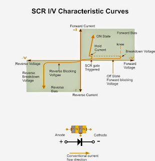
The enforced voltage-current or I-V characteristics curves for the activation of a silicon controlled rectifier may be witnessed in the following image:


Thyristor I-V Characteristics Curves

Thyristor I-V Characteristics Curves


However For a DC input, as soon as the thyristor is triggered ON, due to the explained regenerative conduction it undergoes a latching action such that the anode to cathode conduction holds on and keeps conducting even if the gate trigger is removed.

Thus for a DC power the gate completely loses its influence once the first triggering pulse is applied across the gate of the device ensuring a latched current from its anode to cathode. It may be broken by momentarily breaking the anode/cathode current source while the gate is completely inactive.


 SCR are not designed to be perfectly analogue like the transistor counterparts, and therefore cannot be made to conduct at some intermediate active region for a load which may be somewhere between complete conduction and compete switch OFF.

This is also true because the gate trigger has no influence on how much the anode to cathode can be made to conduct or saturate, thus even a small momentary gate pulse is enough to swing the the anode to cathode conduction into a full switch ON.

The above feature enable an SCR to be compared and considered like a Bistable Latch possessing the two stable states, either a complete ON or  a complete OFF. This is caused due to the two special characteristics of the SCR in response to an AC or a DC inputs as explained in the above sections. 


 How to Use the Gate of an SCR to Control its Switching


 As discussed previously, once an SCR is triggered with a DC input and its anode cathode is self latched, this may be unlocked or switched OFF either by momentarily removing the anode supply source (anode current Ia) fully, or by reducing the same to some significantly low level below the specified holding current of the device or the "minimum holding current" Ih.


This implies that thr Anode to Cathode minimum holding current should be reduced until the thyristors internal P-N latching bond is able to restore its natural blocking feature into action.

Therefore this also means that in order to make an SCR conduct with a gate trigger it's imperative that the anode to cathode load current is over the specified  "minimum holding current" Ih, otherwise the SCR might fail to implement the load conduction, therefore if IL is the load current, this must be as IL > IH.


However as already discussed in the previous sections, when an AC is used across the SCR Anode.Cathode pins, ensures that the SCR is not allowed to execute the latching effect when the gate drive is removed.

This is because the AC signal switches ON and OFF within its zero crossing line which keeps the SCR anode to cathode current to turn off at every 180 degrees shift of the positive half cycle of the AC waveform.

This phenomenon is termed as "natural commutation" and imposes an crucial feature to an SCR conduction. Contrary to this with DC supplies this feature becomes immaterial with SCRs.

But since an SCR is designed to behave like a rectifier diode it responds effectively only to the positive half cycles of an AC and remains reversed biased and entirely unresponsive to the other half cycle of the AC even in the presence of a gate signal. Tis implies that in the presence of a gate trigger, the SCR conducts across its anode to cathode only for the respective positive AC half cycles and stays muted for the other half cycles.

Due to the above explained latching feature and also the cut-of during the other half cycle of an AC waveform, the SCR can be effectively used for chopping phase AC cycles such that the load can be switched at any desired (adjustable) lower power level.

Also known as phase control, this feature can be implemented through an external timed signal applied across the gate of the SCR. This signal decides after how much delay the SCR may be fired once the AC phase has commenced its positive half cycle.

So this allows only that portion of the AC wave to be switched which is being passed after the  gate trigger..this phase control is among the main features of a silicon controlled thyristor.

A Thyristor phase control may be understood by looking at the images below.

The first diagram shows an SCR whose gate is permanently triggered, as may be seen in the first diagram this allows the complete positive waveform to get initiated from start to finish, that from across the central zero crossing line.


Thyristor Phase Control

Thyristor Phase Control


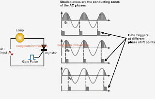
At the outset of each positive half-cycle the SCR is “OFF”. On the induction of the gate voltage activates the SCR into conduction and allows it to be entirely latched “ON” throughout the positive half cycle. When the thyristor is switched on at the start of the half-cycle (θ = 0o), the connected load (a lamp or any similar) would be “ON” for the whole positive cycle of the AC waveform (half-wave rectified AC) at an elevated average voltage of 0.318 x Vp.


As the initialization of the gate switch ON is raised along the half cycle (θ = 0o to 90o), the connected lamp is lighted for a smaller amount time and the net voltage brought to the lamp likewise proportionally less dropping its intensity.

Subsequently it is easy to exploit a silicon controlled rectifier as an AC light dimmer and in many different additional AC power applications for example: AC motor-speed control, heat control devices and power regulator circuits, and so on.

Up till now we have witnessed that a thyristor is fundamentally a half-wave device that is able to pass current in only the positive half of the cycle whenever the Anode is positive and prevents current flow just like a diode in cases where the Anode is negative, even if the gate current remains active.

Nevertheless you may find many more variants of similar semiconductor products to choose from which originate under the title of “Thyristor” designed to operate in both directions of the half cycles, full-wave units, or could be switched “OFF” by the Gate signal.

This kind of products incorporate “Gate Turn-OFF Thyristors” (GTO), “Static Induction Thyristors” (SITH), “MOS Controlled Thyristors” (MCT), “Silicon Controlled Switch” (SCS), “Triode Thyristors” (TRIAC) and “Light Triggered Thyristors” (LASCR) to identify a few, with so many of these devices accessible in many different voltage and current ratings which makes them interesting to be used in purposes at very high power levels.
Thyristor Overview

Silicon Controlled Rectifiers known generally as Thyristors are three-junction PNPN semiconductor devices that could be considered two inter-connected transistors which you can use in the switching of mains operated heavy electrical loads. They are characterized to be latched-“ON” by a single pulse of positive current applied to their Gate lead and can keep on being “ON” endlessly until the Anode to Cathode current is reduced below their specified minimum latching measure or reversed.


Static Attributes of a Thyristor


Thyristors are semiconductor equipment configured to function only in the switching function.
Thyristor are current controlled products, a tiny Gate current is able to control a more substantial Anode current.
Enables current only once forward biased and triggering current applied to the Gate.
The thyristor operates similar to a rectifyier diode whenever it happens to be activated “ON”.
Anode current has to be more than sustaining current value to preserve conduction.
Inhibits current passage in case reverse biased, irrespective of whether or not Gate current is put on.
As soon as turned “ON”, gets latched “ON” performing regardless if a gate current being applied but only in case the Anode current is above latching current.

Thyristors are fast switches which you can use to substitute electromechanical relays in a number of circuits as they simply do not have any vibrating parts, no contact arcing or have problems with deterioration or grime. But additionally to simply switching substantial currents “ON” and “OFF”, thyristors can be accomplished to manage the RMS value of an AC load current without dissipating a considerable amount of power. An excellent example of thyristor power control is in the control of electrical lighting, heaters and motor speed.

In the next tutorial we will look at some basic Thyristor Circuits and applications using both AC and DC supplies.

Automatic Bathroom/Toilet Engage indicator

The post explains a very simple automatic bathroom/Toilet Engage indicator circuit which can be installed with any relevant door bolt for implementing the actions. The idea was created and submitted by Mr. Sandipan.


The Design

Hi Swagatam,

How are doing ? I'm doing good.

I have one more idea that need your help. I would like to implement is at my home ( just a simple useful fun ).

Here is my idea :

Automatic Bathroom/Toilet Engage indicator :

Requirements :
1. If a bathroom/toilet is engaged/ locked from inside ( in use ), a LED indicator ( Placed outside) should glow.
2. If the bathroom/toilet is locked from outside ( Not in use ), the indicator should not glow.
3. The bathroom/Toilet can be locked from inside using one Sliding door bolt or simple door bolt or both.

Based on the above requirement, I design a very simple Circuit using one LED, 2 AA battery and use door locks as switch. Here is the circuit diagram


So, if any bolt or both bolt are used from inside, it complete the circuit and LED will glow.

The problem is, a lot of wiring is visible in back side of the door. I have tested this circuit using breadboard but not with Bathroom/Toilet door :( .

Could you please suggest any other sensor based idea/circuit ?  

Thanks
Sandipan

How to Generate Sinewave PWM

Acquiring a sinewave output from an inverter can be the most crucial and the most advantageous feature for rendering maximum efficiency to the unit, in terms of its output quality.


However achieving a sinusoidal sine wave output could be quite complex and may not be recommended for inverters, because electronic devices normally do not "like" exponentially rising currents or voltages. Since inverters are essentially made by using solid state electronic devices, a sinusoidal waveform is normally avoided. Electronic power devices when forced to operate with sinusoidal waves produce inefficient results since the devices tend to get relatively more hot compared to when operated with square wave pulses.

So the next best option for implementing a sine wave from an inverter is by the way of PWM, which stands for Pulse width modulation.

PWM is an advanced way (digital variant) of putting forth an exponential waveform through a proportionately varying square pulse widths whose net value is calculated to exactly match the net value of a selected exponential waveform, here "net" value refers to the RMS value. Therefore a perfectly calculated PWM with reference to a given sine wave can be used as a perfect equivalent for replicating the given sinewave.  

Furthermore, PWMs become ideally compatible with electronic power devices (mosfets, BJTs, IGBTS) and allow these to run with minimal heat dissipation.

However generating PWMs waveforms is normally considered complex, and that's because the implementation is not easy to simulate in ones mind.

Even I had to go through some brainstorming before I could correctly simulate the function through some intense thinking and imagining.

The best, and the conventional method of generating a sinewaver PWM is by feeding a couple of exponentially varying signals to the input of an opamp for the required processing. Among the two input signals one needs to be much higher in its frequency compared to the other.

The IC 555 can also be used effectively for generating sine equivalent PWMs, by incorporating its built-in opamps and an R/C triangle ramp generator circuit.


The following discussion will help you to understand the entire procedure.


New hobbyists and even the professionals will now find it quite easy to understand regarding how sine wave PWMs are implemented by processing a couple of signals by using an opamp, let's figure it out with the help of the following diagram, and simulation.

As mentioned in the previous section, the procedure involves the feeding of two exponentially varying waveforms to the inputs of an opamp.

Here the opamp is configured as a typical comparator, so we can assume that the opamp will instantly start comparing the instantaneous voltage levels of these two superimposed waveforms the moment these appear or are applied to its inputs.


In order to enable the opamp to implement the required sine wave PWMs correctly at its output, it's imperative that one of the signals has a much higher frequency than the other. The slower frequency here is the one which is supposed to be the sample sine wave which needs to be imitated (replicated) by the PWMs.

Ideally, both the signals should be sinewaves (one with a higher frequency than the other), however the same can be also implemented by incorporating a triangle wave (high frequency) and a sine wave (sample wave with low frequency).

As can be seen in the following images, the high frequency signal is invariably applied to the inverting input (-) of the opamp, while the other slower sinewave is applied to the non-inverting (+) input of the opamp.

In a worst case scenario, both the signals can be triangle waves with the recommended frequency levels as discussed above. Still that would help you to achieve a reasonably good sinewave equivalent PWM.

The signal with the higher frequency is termed as the carrier signal, while the slower sample signal is called the modulating input.


 Referring to the figure above, we can clearly visualize through plotted points the various coinciding or overlapping voltage points of the two signals over a given time span. The horizontal axis signifies the time period of the waveform, while the vertical axis indicates the voltage levels of the two simultaneously running, superimposed waveform.

The figure informs us regarding how the opamp would respond to the shown coinciding instantaneous voltage levels of the two waveforms and produce a correspondingly varying PWM at its output.

The procedure is actually not so difficult to imagine. The opamp simply compares the fast triangle wave's varying instantaneous voltage levels with the relatively much slower sinewave (this can also be a triangle wave), and checks the instances during which the triangle waveform voltage may be lower than the sine wave voltage and responds by instantly creating high logic at its outputs, which is sustained as long as the triangle wave potential continues to be below the sine wave potential, and the moment the sine wave potential is detected to be lower than the instantaneous triangle wave potential, the outputs reverts with a low and sustains until the situation reverts.

This continuous comparison of the instantaneous potential levels of the two superimposed waveforms over the two inputs of the opamps results in the creating of the correspondingly varying PWMs which may be exactly the replication of the sine waveform applied on the non-inverting input of the opamp.

The following image shows the slo-mo simulation of the above operation:


Here we can witness the above explanation being implemented practically, and this is quite how the opamp would be executing the same (although at a much fater rate, in ms).

The upper figure shows a slightly more accurate sine wave PWM depiction than the second scrolling diagram, this is because in the first figure I had the comfort of the graph layout in the background whereas in the second simulated diagram I had to plot the same without the help of the graph coordinates, therefore I might have missed a few of the coinciding points and therefore the outputs looks a little inaccurate compared to the first one.

Nevertheless, the operation is quite evident and distinctly brings out how an opamp is supposed to process a PWM sine wave by comparing two simultaneously varying signals at its inputs as explained in the previous sections.

Actually an opamo would process it much more accurately than the above shown simulation, may be  a 100 times better, producing a extremely uniform and well dimensioned PWMs corresponding to the fed sample. sinewave.

الجمعة، 10 يوليو 2015

Sine Wave Inverter Circuit using Bubba Oscillator

In this post we learn how to make a simple sine wave inverter using bubba oscillator sine wave generator. The idea ws requested by Mr. Ritwik Naudiyal.


The Request 


Hello Sir!! I am a 4th year B.Tech Student Electrical Eng.

We are trying to make pure wave sine wave inverter using PWM and bubba oscillator for our Final project.also along with it a battery charging and auto cut off circuit would be needed

We want the inverter to work for day to day purposes.We would be grateful to you if u can give a working circuit fr this.

thnk u! 


 The Design

The proposed sine wave inverter using bubba oscillator may be understood with the help of the following points:

The stage comprising two 555 ICs are configured as PWM generators where IC1 forms a square pulse generator for the PWMs while IC2 forms the monostable PWM generator with respect to the modulation input applied at its pin5.

The sine wave modulation input at pin5 of IC2 is ahieved with the help of a bubba oscillator created by using four opamps from the IC LM324.

The generated sine wave pulses are fixed at precise 50 Hz and fed to pin5 of IC2 via a BJT common collector for further processing.

The 50 Hz for the bubba oscillator is set by selecting R precisely with the help of the following formula:

f = 1/2(3.14)RC 

IC2 compares the sine wave modulations at its pin5 with the square pulses at its pin2 and generates an equivalent PWM waveform at its pin3.

The flip flop stage reqired for switching the power stage is configured through a single IC 4017 whose outputs are appropriately integarted with the two high gain high current power BJT stage formed by Darlington TIP122 and TIP35.

The pin14 of the 4017 is clocked at around 200 Hz via pin3 of IC1 in order to achieve a 50 HZ switching across the power transistors.

The PWM modulation of the above 50 Hz switching is implemented with the help of the two 1N4148 diodes connected across the bases of the tIP122 and are switched in accordance with the PWM from pin3 of IC1

Assumed waveforms of the PWMs may be referred in the following image:

What's IGBT - How it Works

The insulated-gate bipolar transistor (IGTB) device is a type of three-terminal power semiconductor device which are basically used as electronic switch and is also known for providing a combination of  extremely fast switching and high efficiency in the more newer devices. 

A range of modern appliances such as VFDs (Vaiable Frequency Drives), VSFs (variable speed refrigerators), trains, stereo systems with switching amplifiers, electric cars, and air conditioners use insulated-gate bipolar transistor for switching the electric power. 

Symbol of depletion mode IGBT

In case the amplifiers use insulated-gate bipolar transistor often synthesize waveforms which are complex in nature along with low-pass filters and pulse width modulation; as insulated-gate bipolar transistor are basically design to turn on and off on a fast and rapid pace. 

The pulse repetition rates are boasted by the modern devices which consist of switching application and fall well within the ultrasonic range which are the frequencies which are ten times higher than the highest audio frequency handled by the device when the devices is used in the form of an analog audio amplifier. 

The MOSFETs consisting of high current and characteristics of a simple gate-drive is combined with the bipolar transistors which has low-saturation-voltage capacity by the IGTB. 

A single device is made by IGBT by combining the bipolar power transistor which acts as a switch and an isolated gate FET which acts as the control input. 

The insulated-gate bipolar transistor (IGTB) is majorly used in applications which consists of multiple devices which are placed in parallel to each other and most of the times have capacity of handling very high current which are in the range of hundreds of amperes along with a 6000V of blocking voltage, which in turn is equal to hundreds of kilowatts.use medium to high power such as induction heating, switched-mode power supplies, and traction motor control. Insulated-gate bipolar transistors which are large in size.

Insulated-gate bipolar transistor (IGTB) is a new and recent invention of the time. The first-generation devices which were invented and launched in 1980s and the early years of 1990s were found to have slow switching process relatively and are prone to failure through different modes such as latchup (where the device will continue to be switched on and not turn off till the current keeps on flowing through the device) and secondary breakdown (where when high current flows through the device, a localized hotspot present in the device goes into thermal runaway and as a result burns the device). 

There was a lot of improvement observed in the second-generation devices and the most new devices on the block, the third-generation devices are considered even better than the first tow generation devices. 

The third-generation devices consist of MOSFETs with speed rivaling, and tolerance and ruggedness of excellent level. The devices of second and third generation consists of pulse rating which are extremely high which make them very useful in order to generate large power pulses in various areas such as plasma physics and particle. Thus the second and third generation devices have superseded mostly all the older devices such as triggered spark gaps and thyratrons used in these areas of plasma physics and particle.

These devices also hold attraction for the hobbyist of high-voltage due to their properties of high pulse ratings and availability in the market at low prices. This enables the hobbyist to control huge amounts of power in order to drive devices such as coilgums and Tesla coils.
Insulated-gate bipolar transistors are available at affordable price range and thus act as an important enabler for hybrid cars and electric vehicles.

By Surbhi Prakash

How to Write Codes: PIC Tutorial 11

We dealt with a lot of basics within the last tutorial, therefore I feel the time has come that we composed
our first program.


The program we will write would count the quantity of occasions we turn a switch on, and then exhibit the number. The program would count from 0 to 9, viewable on 4 LEDs in binary form, along with the input or interrupt will likely be on RB0. The number one thing we must conduct is inform the PIC to leap over the address in which the Program Counter points to whenever an interrupt takes place. You will observe that We are employing an unique method of exhibiting hexadecimal numbers. Before I happened apply F9h in which h indicated hexadecimal. We could write this as 0xF9, which is the structure we are going to employ from now on.


Now we need to tell the PIC that we are going to use interrupts, and we are using RB0 pin 6 as an interrupt pin:
bsf INTCON,7;GIE – Global interrupt enable (1=enable)
bsf INTCON,4;INTE - RB0 interrupt enable (1=enable)
I am going to clear the interrupt flag just in case (I never trust anything!)
bcf INTCON,1;INTF - Clear flag bit just in case
Currently we must establish our 2 ports. Keep in mind that as we are now utilizing RB0 as an interrupt pin, this needs to be established as an input:


We are going to use a variable called COUNT to store the number of switch counts. We could just simply increment the value on Port A, but you will see why I am using a variable when we write our interrupt routine.


Therefore, our principal program is composed, and at this point we must inform the PIC how to proceed whenever an interrupt takes place. Within this example, our interrupt will probably be the switch. Just what we would like the PIC to is one to the adjustable COUNT every time the switch is confined. Nevertheless, we just wish to show the how many occasions the switch shuts from 0 to 9. Above, I stated we might be able to have simply incremented the value on Port A every time there is an interrupt. However, Port A has 5 bits, in case we simply incremented the port, we are going to possess the highest count of 31. There are a couple of explanations why I selected not to move up to 31.

Initially, we will employ a 7-segment screen, which could at the most only go from 0 to 15 (0 to F in hex). Next, I additionally wish to show you a few of the arithmetic commands which you stumbled on in the past few lessons. Therefore we will continue with our interrupt routine. Currently the firstly we must accomplish is briefly store the details of our w register, since we have been applying this to shift the contents of COUNT to PORTA. In case we don’t save it, in that case we might be able to deliver a totally different number because of our arithmetic. Therefore let’s accomplish that first:


At this point we we understand if the value of COUNT is 9 or more. Just what we need to accomplish now is if COUNT is more than 9, place it back to 0, or else return to the main program to ensure that we are able to deliver it to Port A. The BTFSS command since you understand would the subsequent
instruction in case the carry flag is scheduled i.e COUNT = 10:


The only thing which is remaining to do now is enter collectively as well as determine values to our constants, which we are able to perform right at the start of our program.
Each time you activate the switch on, the LEDs are going to count up in binary from 0000 to 1010
then back to 0000.


The following figure shows the circuit diagram compatible with the above explained code. Interestingly you will find that the timing capacitor has been included in the design. This is nice little ploy through which you get the freedom of avoiding the inclusion of the capacitor in case you don't have any with you during that time.
Here the capacitance comes into play via the stray capacitance across the oscillator pin and ground.
Of course it might not seem to be a very intelligent way of avoiding a capacitor practically since the stray value might vary with different given conditions.
Another section which can be witnessed in the circuit is the denouncing network across the switch. This prevents interference while mechanical switching and prevents the PIC from getting confused if the switching was a single toggle or multiple toggles.

Understanding Interrupts: PIC Tutorial 10

The topic of interrupts may well gonna be the lengthiest and toughest to go thru. You cannot find any uncomplicated method of detailing interrupts, however with a little luck towards the end of this part you may be able to apply interrupts into your own programs.


We have separated the section into 2 stages. That is to enable separate the topic into sections, also to provide you with an handy plit up for easy understanding. What exactly is an interrupt? Surely, as the term indicates, an interrupt is a technique or a signal that prevents a microprocessor/microcontroller from whatever thing its performing that something different could happen. Allow me to give you an daily illustration. Think you are relaxing in your own home, conversing to another person. All of a sudden the phone sounds. You quit talking, and grab the telephone to talk to the caller. Once you have your telephone interaction, you decide to return to conversing to the individual before the telephone rang. It is possible to consider the principal routine while you chatt to somebody, the phone ringing brings about to disrupt your conversing, and the break in routine is the method of speaking on the phone. While the phone discussion comes to an end, then you go back to your primary routine of chatting. This illustration is precisely how an interrupt a processor to take action. The primary program is operating, carrying out certain function in a circuit, however when an interruption takes place the primary program halts while a different routine is performed. routine ends, the processor moves back to the primary routine just as before. The PIC possesses 4 sources of interrupt. They could be broken down into a couple of groups. Two are sources of interrupts which can be utilised outwardly to the PIC, whilst the other two are inner processes. Let me clarify the two external types here. The other two is going to be described in different tutorials once we arrive at timers and storing data. Should you check out the pin-out of the PIC, you will notice that pin 6 it is RB0/INT. At this point, RB0 is clearly Port B bit 0. The INT represents that it could as well be configures as an outside interrupt pin. Furthermore, Port B pins 4 to 7 (pins 10 to 13) may also be utilized for interrupts. Before we are able to employ the INT or another Port B pins, we must accomplish two tasks. Very first we must inform the PIC that we will utilize interrupts. Next, we must designate which port B pin we are going to be utilising as an interrupt rather than as an I/O pin. Inside the PIC you can find a register known as INTCON, and is at address 0Bh. In this register you will discover 8 bits that may be enabled or disabled. Bit 7 of INTCON is known as GIE. This is the Global Interrngupt Enable. Fixing this to 1 informs the PIC that we will employ an interrupt. Bit 4 of INTCON is known as INTE, INTerrupt Enable. Putting this bit to 1 conveys to the PIC that RB0 is going to be an interrupt pin. Configuring bit 3, called RBIE, informs the PIc that we are going to be utilizing Port B bits 4 to 7. At this point the PIC understands when this pin can be high or low, have to halt what it’s performing and proceed with an interrupt routine. At this point, we must inform the PIC whether or not the interrupt will likely be on the ascending edge (0V to +5V) or the dropping edge (+5V to 0V) transformation of the signal. Put simply, do we wish the PIC to interrupt each time the signal moves from low to high, or from high to low. By delinquency, this can be established to be placed on the rising edge. The edge ‘triggering’ is scheduled up in an additional register called the OPTION register, at address 81h. The bit we are enthusiastic about is bit 6, often referred to as INTEDG. Setting this to 1 triggers the PIC to disrupt on the mounting edge (default state) and setting it to 0 stimulates the PIC to disrupt on the sliding edge. If you would like the PIC to activate on the rising edge, then you certainly don’t have to do anything to this bit. At this point, sadly, the Option register is in Bank 1, meaning that we enjoy to modify from bank 0 to bank 1, set the bit in the Option register, after that return to bank 0. The key here is to accomplish every bit of the Bank 1 registers in a single strike, for example establishing the port pins, after that returning to Bank 0 if you are done. Fine, consequently we have notified the PIC which pin will probably be the interrupt, and where edge to trigger, what goes on in the program and the PIC any time the interrupt happens? A couple of stuff take place. Very first, a ‘flag’ is scheduled. This informs the internal processor of the PIC that an interrupt has transpired. Next, the program counter (which I talked about within the previous tutorial) tips to a specific address within the PIC. Let’s swiftly check out all these individually. Interrupt Flag In our INTCON register, bit 1 is the interrupt flag, called INTF. At this point, whenever any interrupt arises, this flag will likely be fixed to 1. When there isn’t an interrupt, the flag is placed to 0. As well as that is just about all accomplishes. At this point you may be pondering ‘what is the point?’ Surely, even though this flag is scheduled to 1, the PIC is not able to, and will not, react to another interrupt. Therefore, let’s express that we bring about an interrupt. The flag will likely be fixed to 1, and the PIC might go to our routine for working the interrupt. When this flag wasn’t fixed to 1, and the PIC was permitted to continue answering the interrupt, then continuously pulsing the pin could keep the PIC returning to the beginning of our interrupt routine, and by no means completing it. Returning to my illustration of the telephone, it’s similar to lifting the telephone, and immediately once proceeding to discuss it begins ringing yet again since another person wishes to speak with you. It is advisable to complete one dialogue, then grab the phone again to speak with the subsequent individual. You can find a small problem with this flag. Even though the PIC quickly sets this flag to 1, it doesn’t set it again 0! That activity must be exercised by the programmer – i.e. you. This can be effortlessly accomplished, since I’m certain presume, and needs to be achieved after the PIC has carried out the interrupt routine.

Memory Location

Whenever you initially power up the PIC, or in case there exists a reset, the Program Counter tips to address 0000h, that could be immedaitely at the outset of the program memory. But, in the event there is an interrupt, the Program Counter would indicate address 0004h. Therefore, while we are composing our program that will have interrupts, we firstly must inform the PIC to hop over address 0004h, and maintain the interrupt routine which begins at address 0004h discrete from the remainder of the program. This can be hassle-free to perform. Initially, we commence our program with a command known as ORG. This command indicates Origin, or start. We stick to it with an address. Since the PIC commences at address 0000h, we type ORG 0000h. After that we must bypass over address 0004h. We accomplish this by putting a GOTO instruction, accompanied by a label which tips to our primary program. We after that adhere to this GOTO command with one more ORG, this moment with the address 0004h. It will be after this command that we insert our interrupt routine. At this point, we might be able to possibly type in our interrupt routine straight following the second ORG command, or we are able to position a GOTO statement which points to the interrupt routine. It truly is related to option on your part. To inform the PIC it offers arrived at the conclusion of the interrupt routine we must position the command RTFIE towards the end of the routine. This command signifies return from the interrupt routine. While the PIC notices this, the Program Counter indicates to the final position the PIC was at before the interrupt occurred. We have established below a brief section of code to display the above:


There are a couple of stuffs you should be informed when utilizing interrupts. The initial tends to be that if you might be utilizing the identical register in your primary program and the interrupt routine, in mind that the details of the register will most likely alter when the interrupt takes place. For instance, let’s utilizing the w register to forward data to Port A primary program, therefore you can be additionally utilizing the w register in the interrupt routine to shift data from one destination to another. In case you are not cautious, the w register would include the last value it received while it had been in the interrupt routine, so when you return from the interrupt this information is going to be delivered to Port A rather than the value you possessed before the interrupt occurred.

The means around this is to momentarily save the details of the w register prior to when you utilize it once again in the interrupt routine. The second is the fact you can find a delay between when one interrupt takes place and when the subsequent one can arise. While you understand, the PIC possesses an exterior clock, which could possibly be a crystal or it could be a resistor-capacitor combo. No matter what the frequency of this clock, the PIC divides it by 4 after which employs this for it’s inner timing. For instance in case you have a 4MHz crystal linked to your PIC, in that case the PIC would perform the instructions at 1MHz. This interior timing is known as an Instruction Cycle. At this point, the data sheet claims (undoubtedly in diminutive print) that you need to enable 3 to 4 instruction rounds between interrupts. My would be to enable 4 rounds. The reason behind the delay is the PIC requires time to leap to the interrupt address, the flag, and arrive back away from the interrupt routine. Therefore, keep this in your mind if you work with an alternate circuit to activate an interrupt for the PIC. At this point, a point to is the fact that if you utilize bits 4 to 7 of Port B as an interrupt. You are unable to choose specific pins on Port B to function as an interrupt. Therefore, in case you allow these pins, they likely could be all obtainable. Therefore, for instance, you can’t simply have bits 4 and 5 – bits 6 and 7 will likely be empowered at the same time. What exactly is the purpose of getting four bits to represent an interrupt? Surely, you might have a circuit hooked up to the PIC, in case anyone of four lines go high, in that case this may be an issue that you require the PIC to influence instantly. One illustration of this could be a home security alarm, in which four sensors are linked to Port B pins 4 to 7. Any specific sensor can prompt the PIC to trigger an alarm, and the alarm signaling routine is the interrupt routine. This spares checking the ports constantly and permits the PIC to continue with different matters. Within the next tutorial, we are going to compose a program to manage an interrupt.

Understanding Data Tables: PIC Tutorial 9

There exists a great option in the training set that permits you to make use of a data table.
A data table is just a list of data quotes, in which all is looked over based on a few considerations.


For instance, you could have a circuit that utilizes a PIC which counts the quantity of instances an input pin becomes high in 1 second. After that you can exhibit the number on a 7 segment display. As soon as the timing has launched, the PIC starts counting the quantity of occasions the pin goes high. After 1 second it visits the table and glances up the data it must display the number on the display that symbolizes the amount of situations the pin got high. This can be beneficial, since we don’t determine what the figure could be until the PIC has accomplished its estimate. By utilizing a table, we are able to allow the PIC determine which figure to portray. At this point, before I continue to show you how the data table functions, I might have to tell you that the PIC maintains path of whereabouts in the program it is whilst the program is operating. It facilitates for those who have performed certain programming in BASIC. Otherwise, don’t be anxious, you might want to continue to learn about the theory. Envision there is a BASIC program similar to the one presented below:

10               LET K=0
11               K=K+1
12               IF K>10 THEN GOTO 20 ELSE GOTO 11
20                     PRINT K
21                     END

The program begins at line 10. As soon as K is scheduled to 0, it next advances to line 11. After we have included 1 to K we after that proceed to line 12. At this point we might be curious if K is higher than 10. In case it is, next we head to line 20, or else we return to line 11. Line 20 documents the K, and line 21 concludes the program. BASIC employs line statistics to assist the programmer keep a record of where issues are, as labels are not authorized. The PIC employs labels to escape between destinations – or can it really? We utilize the labels to ensure that we be aware of where issues are, as well as to ensure we are able to inform the PIC in a simple way where to search. Precisely what occurs is the PIC takes advantage of an inner line counter called a Program Counter. The Program Counter (abbreviated to PC) trail of the memory destination of where the present instruction is. Whenever we inform the PIC to visit a selected label, it understands the memory spot and therefore augments the PC until it sees that memory destination. This is precisely the same method as we check out the BASIC program above. Below is a segment of code, with the memory spaces, or the items of the PC, beside every instruction:

PC Instruction

0000             movlw 03
0001             movwf 0C
0002  Loop    decfsc 0C
0003              goto Loop
0004  end

In the demonstration above, We have fixed the PC to 0000. On this we have the instruction movlw 03. When the PIC has implemented this data, it increments the PC in order that the subsequent instruction is scanned. At this point the PIC views movwf 0C. The PC is incremented yet again. Now the PIC studies decfsc 0C. In case the details of 0C are not 0, in that case the PC is incremented by 1, as well as the following instruction, goto Loop, informs the PC to return to position 0003, which there is the said Loop. In case the details of 0C is 0, then the PC is advised to increment by 2, put simply omit the subsequent instruction. This places the PC at position 0004, wherein the program finishes. The destinations are fixed by the assembler, and we don’t generally ought to be concerned what the PC is accomplishing. Until, we find the need to bring it under control just like while we do when utilizing data tables. The most convenient way to describe how a data table functions, is to begin with an illustration.

PC equ  02
movlw  03
call        table
             :
table      addwf PC
retlw      01
retlw      02
retlw      03
retlw      04
retlw      05
retlw      06
retlw      07
return
The initial instruction is allocating the label PC with the address of the Program Counter (02h). We will be soon after putting the value of 03h into the w register. We after that communicate to table. The foremost line in the subroutine table augments the details of the W register (03h) to the program counter. This triggers the program counter to raise by 3, or to put it a different way, stimulates the program counter to proceed down 3 lines. While the counter arrives 3 lines down it the PIC recognizes the instruction retlw. This command sends the value following it into the W register, after which comes back from the subroutine. RETLW basically signifies Return, Literal to W. See I placed a comma after the word Return. Since we are in a subroutine, we require a Return instruction to surface of it. Therefore the RET in the instruction. After the RETLW instruction is a number, and this is exactly what is put into the W register. In this instance it is the figure 3. We could designate any quantity to the W register, so long as this figure is combined with the Program Counter in the table subroutine, we are going to discover a retlw instruction. In the above illustration this implies we are able to possess any number from 1 to 7. In case we proceed past the subroutine, we might be able to finish up performing an additional section of the program. For this reason, it is usually a smart move to place the data table exactly towards the end of the PIC program, therefore if we do overshoot in that case we are going to arrive at the conclusion of the program anyhow.

Understanding Bit Operations: PIC Tutorial 8

Bit functions permit us to shape a single bit within a expression. They permit us to proceed,
set and get rid of single bits in registers or numbers that we stipulate.


PIC Tutorial - 7......................................PIC Tutorial - 9
At the conclusion of this course We will disclose a program designed to create a set of sequencing lights that proceed forward, then the reverse way. We observed this accomplished earlier when we examined the exclusive OR function, wherein we Exclusively ORed the ports with a expression. We have uptil now noticed a few bit functions when we establish the ports on the PIC, and

Let me reiterate their utilization here.
BCF

This instruction will wipe of a bit that we stipulate in a register that we designate. The syntax
is:
BCF      <register>,<bit>

We employed this earlier to alter from page 1 to page 0 by removing a bit in the STATUS register. We are able to likewise use it to fix a bit to 0 in any different register/location. For instance, in case we wished to set the 3rd bit in 11001101 saved in section 0C to 0, we might insert:

BCF 0C,03

BSF

This instruction would fix any bit we stipulate to 1 in any register that we indicate. We utilized this earlier to proceed from Page 0 to Page 1. The syntax is: BSF <register>,<bit>, and is utilized in precisely the same method as BCF above.

BTFSC

Up to now we could set or clear a bit in a register. However imagine if we need to basically check if a bit is a 1 or a 0 in a register? Surely, it is possible to use BTFSC. It states Bit Test Register F, and Skip If It Is Clear. This instruction is going to analyze the bit we designate in the register. In case the bit is a 0, the instruction would inform the PIC to by pass the subsequent instruction. We might utilize this instruction in case we wished to check a flag, for example the carry flag. This spares us needing to read the STATUS register and searching for the individual bits to learn which flags are fixed. 29 For instance, in case we wished to check if the Carry flag was set to 1 after we had added 2 figures, then we could type the following:

BTFSC           03h,0
carry on here if set to 1
or here if set to 0

In case the status of the bit is a 1, in that case the instruction subsequent to BTFSC would be completed. In case it is set to a 0, in that case the subsequent instruction is skipped. The following part of code exhibits in which it might be employed:
Loop    :
            :
            :
            BTFSC 03,0
            Goto Loop

In the above code, the PIC will simply get out of the loop in case bit 0 of the STATUS register (or the Carry flag) is defined to 0. Or else, the goto command would be conducted.

BTFSS

This instruction states Bit Test Register F, And Skip If Set. This can be comparable to the BTFSC instruction, apart from that the PIC would omit the subsequent instruction if the bit we have been evaluating is set to 1, instead of 0.

CLRF

This instruction would fix the whole details of a register to 0. The syntax is:

CLRF <register>
We employed this earlier to set the output of the Ports to 0, by applying CLRF 85h. We furthermore employed it to fix the Ports to include all pins to output by utilizing CLRF 05h.

CLRW

This could be resembling the CLRF instruction, except for clears the W register. The syntax is pretty simply:

CLRW

RLF And RRF

These directions would transport a bit in a register a single slot to the left (RLF) or the right (RRF) in a register. For instance, if we needed 00000001 and we employed RLF, in that case we might possess 00000010. At this point, what goes on in case there is 10000000 and applied the RLF instruction? Surely, the 1 would be positioned in the carry flag. In case we applied the RLF instruction once more, the 1 would reappear back at the start. The alike occurs, however in opposite, for the RRF instruction. The case in point below shows this for the RLF instruction, in which We have can see the 8 bits of a register, as well as the carry flag:
                            C 87654321
                            0 00000001
RLF                     0 00000010
RLF                     0 00000100
RLF                     0 00001000
RLF                     0 00010000
RLF                     0 00100000
RLF                     0 01000000
RLF                     0 10000000
RLF                     1 00000000
RLF                     0 00000001

Example Program

We are now gonna see an example code that one can compile and drive. It would generate a sequencing light beginning at PortA bit 0, going to PortB bit 8 and then returning.
Hook up LEDs to each one of the Port pins. We will have some of the bit procedures pointed out in this tutorial.

TIME EQU 9FH             ; Variable for the delay loop.
PORTB EQU 06H           ; Port B address.
TRISB EQU 86H             ; Port B Tristate address.
PORTA EQU 05H           ; Port A address.
TRISA EQU 85H             ; Port A Tristate address.
STATUS EQU 03H         ; Page select register.
COUNT1 EQU 0CH       ; Loop register.
COUNT2 EQU 0DH       ; Loop register.

BSF STATUS,5            ; Go to page 1
MOVLW 00H                ; and set up
MOVWF TRISB            ; both Ports A and B
MOVLW 00H                ; to output,
MOVWF TRISA            ; then return to
BCF STATUS,5             ; page 0.
MOVLW 00H                 ; Clear Port A.
MOVWF PORTA           ;

    ; Start of main program

RUN
MOVLW 01H              ; Set the first bit
MOVWF PORTB       ; on Port B.
CALL DELAY              ; Wait a while
CALL DELAY               ;

; Move the bit on Port B left, then pause.

RLF PORTB,1
CALL DELAY
CALL DELAY
RLF PORTB,1
CALL DELAY
CALL DELAY
RLF PORTB,1
CALL DELAY
CALL DELAY
RLF PORTB,1
CALL DELAY
CALL DELAY
RLF PORTB,1
CALL DELAY
CALL DELAY
RLF PORTB,1
CALL DELAY
CALL DELAY
RLF PORTB,1
CALL DELAY
CALL DELAY
RLF PORTB,1           ; This moves the bit into the carry flag

; Now move onto Port A, and move the bit left.

RLF PORTA,1            ; This moves the bit from the zero flag into PortA

CALL DELAY
CALL DELAY
RLF PORTA,1
CALL DELAY
CALL DELAY
RLF PORTA,1
CALL DELAY
CALL DELAY
RLF PORTA,1
CALL DELAY
CALL DELAY

; Move the bit back on Port A

RRF PORTA,1
CALL DELAY
CALL DELAY
RRF PORTA,1
CALL DELAY
CALL DELAY
RRF PORTA,1
CALL DELAY
CALL DELAY
RRF PORTA,1             ; This moves the bit into the zero flag

; Now move the bit back on Port B

RRF PORTB,1
CALL DELAY
CALL DELAY
RRF PORTB,1
CALL DELAY
CALL DELAY
RRF PORTB,1
CALL DELAY
CALL DELAY
RRF PORTB,1
CALL DELAY
CALL DELAY
RRF PORTB,1
CALL DELAY
CALL DELAY
RRF PORTB,1
CALL DELAY
CALL DELAY
RRF PORTB,1
CALL DELAY
CALL DELAY             ; Now we are back where we started,
                                     ;
GOTO RUN                 ; let's go again.

Understanding Logical and Arithmetic Operators: PIC Tutorial 7

Below, we will analyze how you can wiggle individual bits, carry out certain straightforward
arithmetic, as well as data tables.

Logical Managers

Within the last tutorial I presented the Exclusive OR operation. The ExOR function is understood as a logical operator. Within this tutorial I will enlighten the additional logical operators that the PIC promotes. There won’t be any kind of case in point programs, however We will learn easy methods to use the operators by applying small areas of code. AND The AND function basically analyzes two bits and delivers a 1 whether they are the same, and a 0 in case they are distinctive. For instance, if we mentioned 1 AND 1, the outcome is 1, while in case we declared 1 AND 0 the consequence would be 0. Needless to say, we are able to evaluate words also, as well as all of the the AND function accomplishes is review the two terms bit by bit. The instance below demonstrates two 8-bit words becoming ANDed together with the product:

              11001011
AND      10110011
Equals     10000011

I hope you agree, the outcome will simply possess a 1 whenever 2 1s hand in hand with one another in the a pair of words. We are able to utilize the AND function to verify the ports, for instance. In case we are checking a few I/O pins that are linked to a circuit, and we should keep an eye on a particular situation in which only a few of the pins are high, in that case we are able to pretty much read the port, after which AND the outcome with the condition we have been examining for, identical to the instance above. The PIC provides us two ingredients for AND.
They are ANDLW and ANDWF. ANDLW permits us to carry out an AND function with the details of the W register, and a amount that we stipulate.
The syntax is: ANDLW <number> wherein <number> is exactly what we are going to AND the contents of W with. The consequence of the AND function would be stored directly into the W register.
ANDWF permits us to carry out an AND function on the W register and a different register, for example a PORT. The syntax is: ANDWF <register>,d in which <register> is the register we are enthusiastic about, e.g. PORTA, and d shows the PIC where you should position the result. If d=0, the outcome is put in the W register, and of d=1 the end result is saved in the register we stipulated. The two parts of code below display a good example of each AND function. The initial is examining the status of the PORTA, in which we need to check if the inputs are 1100. We can place the outcome back into the W register

movlw         1100
ANDWF     05h,0

The second illustration might now verify the contents of the W register:
ANDLW     1100

OR

We have by now discovered one OR function, to be precise the XOR. This develops into a 1 if two bits are not the same, but are different. You can find another OR function called IOR, which is the inclusive OR. This function will generate a 1 in case either bit is a 1, but additionally if each bits are 1. Below is a clear-cut truth table to illustrate this:
A   B   O/P
0    0     0
0    1     1
1    0     1
1    1     1
Arithmetic Operators

ADD 

This function accomplishes what usually it claims. It contributes two figures! In case the consequence of adding the two figures surpasses 8 bits, in that case a CARRY flag will probably be set. The CARRY flag is situated at address 03h bit 0. When this bit is scheduled, then the two figures surpassed 8 bits. When it is a 0, in that case the consequence is located within 8 bits. As before, the PIC delivers us two styles of ADD, specifically ADDLW and ADDWF. As you might have assumed, this is quite like the above function. ADDLW offers the contents of the W register to that we stipulate. The syntax is: ADDLW <number> ADDWF add the contents of the W register and some other register that we designate. The syntax is: ADDWF <register>,d is where <register is the register we specify and d tells the PIC where to place the outcome. If d=0, the result is put in the W register, and is d=1 it set up in the register that we selected.

SUB

At this point, I guess you can’t presume what this function conducts! Indeed, you suspected it, this function
subtracts one bit from another. Again the PIC provides us 2 tastes: SUBLW and SUBWF. The syntax is precisely the similar to for the ADD function, apart from evidently you type SUB in place of ADD!

Increment 

In case we wished to include 1 to a number in the PIC, we could absolutely make use of the ADD function, and utilize the number one. ~The difficulty with this is that we must first place the figure into the W register, subsequently use ADDLW 1 control to increment it. In case we desired to include 1 to a register, it can be worse still. We first must place the number 1 into the W register, after that use ADDWF <register>,1. Therefore, for instance, to include 1 to location 0C, say, we would need to possess the following part of script:

movlw    01
addwf     0c,1

There exists an easier method of conducting this. We can exercise the command INCF. The syntax is: INCF <register>,d where <register>, is the register, or place, that we are concerned in, and d shows the PIC where you should position the outcome. In case d=0, the outcome is within the W register, and in case d=1, the consequence is set in the register we stipulated. By utilizing this individual instruction we are able to actually fifty percent of the coding. In case we desired the outcome restored into the W register, in that case employing the instance above, we might have had to include an additional command to shift the items of 0C back into the W register, after which place the 0C register back to no matter what it was. There exists increment command. It is INCFSZ. This command might increment the register that we stipulate, however if we the register equals 0 after the increment (that will occur while we include 1 to 127) after that the PIC will probably by pass the subsequent instruction. The portion of code below reflects this:

Loop         incfsz            0C
                 Goto Loop
                 :
                 :
Remainder of program.

In the above portion of code, 0C is going to be incremented by 1. We next own an instruction that informs the PIC to return to our tag named Loop, and increment 0C by 1 again. This continues until 0C equals 127. In this circumstance, when we increment 0C by 1, 0C is going to now match 0. Our INCFSZ instruction could very well inform the PIC to omit the subsequent instruction, which in this instance is the goto declaration, hence the PIC will go forward with the remaining of the program.

Decrement

We have by now discussed the decrement function in earlier training, therefore I won’t revise
it anymore.

Compliment

The final instruction in this discussion would reverse every single bit in the register that we stipulate. The syntax is: COMF <register>,d wherein <register is the register that we wish to reverse, and d will inform the PIC where to collect the result. If d=0, the result is saved in the W register. If d=1, the result is saved again into the register we assigned. The following example exhibits this instruction in practicality: 
0C = 11001100
COMF 0C,1
0C = 00110011

This could be utilized, for instance, to swiftly swap the pins of a port from output to input and so on.

Using Memory Space Efficiently: PIC Tutorial 6

Up till now, we have composed the PIC blink an LED on and off. Subsequently we were capable of
with our PIC by including a switch, therefore varying the flash speed.


The sole issue is, the program is quite lengthy and rather inefficient of memory space. It seemed ok while i was including the commands for the first time, however there ought to be an easier way of executing it. Positively there is, we will analyze how we were literally switching the LED on and off.

movlw          02h
movwf          PORTA
movlw          00h
movlw PORTA

At first we stuffed our w register with 02h, after that transfered it to our PortA register to switch the
LED on. To switch it off, we packed w with 00h after which shifted it to our PortA register. Inbetween all these routines we were forced to get in touch with a subroutine to ensure that we could observe the LED
flashing. Therefore, we needed to transfer two sets of info a couple of times (one time into the w register then to
PORTA) as well as call a subroutine two times (once for on then once for off).
Thus, how could we achieve this with added efficiency? Very simple. We utilize a different instruction known as
XORF.
The XORF instruction works an Exclusive OR function on the register that we stipulate with the info we provide. I believe I have to clarify what in the world an Exclusive OR is before we continue.
In case we have two inputs, and one output, the input can only be a 1 if, and as long as, the two inputs differ. While they are the same, then the output will probably be 0. The following is a truth table, for individuals who choose to check out these:

A          B            F
0           0            0
0           1            1
1           0            1
1           1            0

We will at this point check out what goes on if we render B the just like our earlier output, and simply
altering the value of A:
A           B          F
0            0          0
0            0          0
1            0          1
1            1          0
1            0          1

If we maintain the value of A same as 1, and we Exclusive OR it with the output, the output would toggle. In case you can’t notice this from the truth table, below it can be witnessed utilizing binary:

                        0       Current Output
EX-OR With 1 1       New Output
EX-OR With 1 0       New Output

Maybe you can find that by exlusive ORing the output with 1, we will be now toglling the output from 0 to 1 to 0.
Hence, to switch our LED on and off, we only require a couple of sentences:
MOVLW     02h
XORWF      PORTA,1
What precisely we will be accomplishing is adding our w register with 02h. We are in that case Exclusive ORing this number with no matter what is on our PortA. In case bit 1 is a 1, it is going to alter to a 0. In case bit 1 is a 0, it is going to alter to a 1.
Let’s examine this code once or twice, to display how it's running binary:
                      PORTA
                      00010
xorwf               00000
xorwf               00010
xorwf               00000
xorwf               00010

We don’t actually have to load the identical value into our w register every time, therefore it is possible to accomplish this one time at the start, and simply leap back to our toggle command. Additionally, we don’t
ought to fix a value on our PortA register. The reason? Surely, since in case on power up it is a 1, we can easily toggle it. I, alternatively a 0 on power up, we would even now toggle it.

Therefore you would want to see our newly formed code. The first one represents our blinking LED code, while the second shows the one with the addition of the switch:


Lets wish you can find that simply by making use of one easy instruction, we now have cut down the scale of
our program. The truth is, in order to display just how much we could reduce our programs by, We have demonstrated the two programs, just what were composed, and their dimensions in the table below:
Program               Alter                           Dimensions (Bytes)
Flashing LED         Original                             120
Flashing LED         Subroutine Added          103
Flashing LED         XOR Function Used       91
LED With Switch   Original                           132
LED With Switch   XOR Function Used       124.


Therefore, not just have we discovered a few novel instructions, we certainly in addition have decreased the size of our scripting!